

AI Infrastructure series · Part 6 of 24
Part 5 showed that splitting a model across GPUs only works if the GPUs can swap data almost instantly. NVLink is how NVIDIA makes that possible: a direct, very wide connection between GPUs that skips the CPU entirely. This part counts the bytes that actually move for each token, follows a packet over PCIe and over NVLink, explains what NVSwitch adds, walks through an all-reduce step by step, and shows how to check the wiring of a real server before you put a model on it.
Race the same AI job over PCIe, NVLink 4, NVLink 5 and InfiniBand, watch a ring all-reduce move chunks between GPUs, explore three server topologies, and work out how much of each token’s time goes on talking rather than computing.
What is NVLink, and why do GPUs need to talk at all?
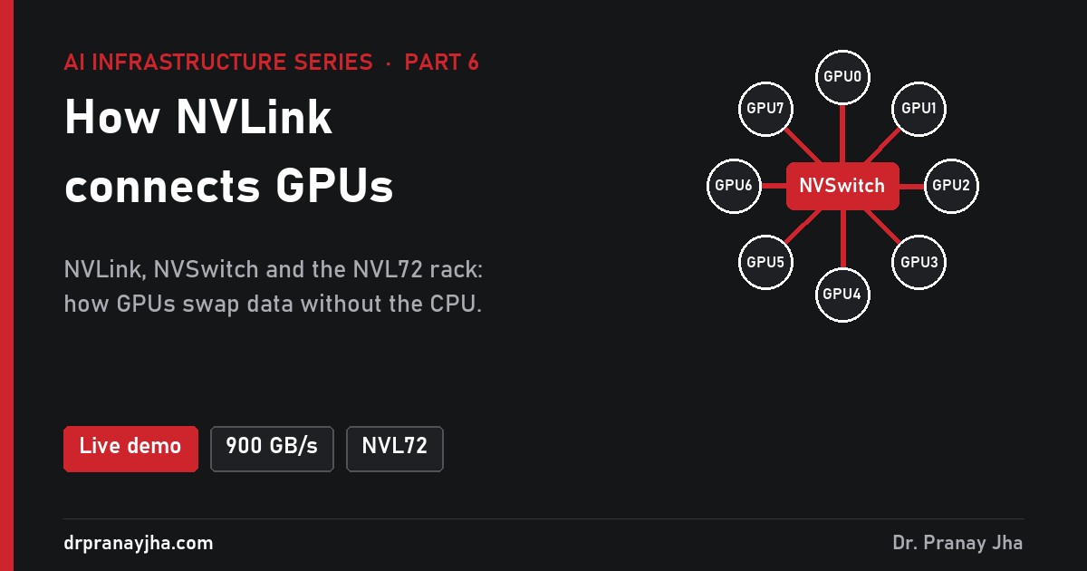
NVLink is a connection that NVIDIA builds into its data centre GPUs so they can send data straight to each other. A normal graphics card talks to the rest of the computer through a PCIe slot, and if two cards want to swap data, it travels up through the PCIe connections and back down. NVLink is a separate, much faster road that goes directly from GPU to GPU.
A single GPU never needs it. The need starts the moment one job runs on more than one GPU, because each GPU then holds only part of the picture and must regularly get the rest from the others. There are four kinds of traffic, and each one stresses the link differently:
Tensor-parallel all-reduce. When each layer is sliced across GPUs (part 5), every GPU computes a partial result, and the partial results must be summed before the next layer can start. That happens twice per layer, for every token. Many small, urgent messages: delay matters as much as bandwidth.
Pipeline hand-offs. When whole groups of layers live on different GPUs, the activations for each token are passed from one stage to the next. One message per stage per batch, so this traffic is light and can cross a slower link.
Mixture-of-experts all-to-all. In an MoE model (part 12), each token is sent to the GPUs holding its chosen experts and the results are sent back, twice per MoE layer. Every GPU talks to every other at once, so the wiring pattern matters, not only the speed.
KV cache and gradient transfers. Serving systems that split prefill and decode move a conversation’s KV cache (part 14) between GPUs, often gigabytes at a time. Training averages every gradient across GPUs after every step. Large, bulk messages: here bandwidth is everything.
Tensor parallelism and expert parallelism are the two that force the choice of hardware. They run inside every forward pass, so if the link is slow, every token is slow.
How many bytes move for each token?
Take Llama 3.1 70B, split 8 ways with tensor parallelism. It has 80 layers and a hidden size of 8,192. Each layer ends its attention block and its MLP block with an all-reduce over the hidden vector, so the sums below are exact for the model’s shape. The timings use illustrative per-message delays (8 µs on NVLink with NVSwitch, 30 µs over PCIe), which are typical orders of magnitude, not measurements.
One message. One token’s hidden vector in 16-bit: 8,192 numbers × 2 bytes = 16 KB.
Messages per token. 2 all-reduces per layer × 80 layers = 160 all-reduces for every token the model writes.
Bytes each GPU sends per all-reduce. A ring all-reduce over 8 GPUs makes each GPU send 2 × 7/8 of the message (explained further down): 28 KB.
Bytes per token. 160 × 28 KB = about 4.5 MB sent by each GPU for one token, and the same amount received.
Time on NVLink 4. 4.5 MB ÷ 450 GB/s each way = 10 µs of transfer, plus 160 × 8 µs = 1.28 ms of per-message delay. About 1.3 ms per token.
Time on PCIe 5.0. 4.5 MB ÷ 64 GB/s = 70 µs of transfer, plus 160 × 30 µs = 4.8 ms of delay. About 4.9 ms per token.
Now compare that with the useful work. Each of the 8 H100s holds 140 GB ÷ 8 = 17.5 GB of weights and must read them once per decode step: 17.5 GB ÷ 3.35 TB/s = 5.2 ms (part 4). With NVLink, talking adds 1.3 ms to a 5.2 ms step. Over PCIe it adds 4.9 ms, nearly doubling the time per token.
The picture changes with batch size and with prefill. In decode, a batch of 64 users makes each message 64 times bigger; in prefill, a 2,000-token prompt makes it 2,000 times bigger. Bandwidth then takes over from delay:
| Situation (70B, 8-way TP) | Sent per GPU per forward pass | NVLink 4 | PCIe 5.0 | Main limit |
|---|---|---|---|---|
| Decode, 1 user | 4.5 MB | 1.3 ms | 4.9 ms | per-message delay |
| Decode, batch of 64 | 294 MB | 1.9 ms | 9.4 ms | both |
| Prefill, 2,000-token prompt | 9.2 GB | 22 ms | 148 ms | bandwidth |
Two lessons come out of this. Tensor parallelism over PCIe is possible but costly: the GPUs spend a large share of every step waiting. And a faster link helps most when messages are large (big batches, long prompts, training), while a low-delay switch helps most when they are small. NVLink with NVSwitch provides both.
How does data travel over PCIe and over NVLink?
In a server without NVLink, every GPU sits in a PCIe slot. The slots hang off PCIe switches, which hang off the CPU’s root complex, and in a two-socket server half the GPUs belong to the other CPU. A message from GPU 0 to GPU 3 climbs from the card to its switch, up to its CPU, across the socket link to the other CPU, and back down. Each hop adds delay, and every hop is shared with network cards, storage and anything else on that CPU.
Same message, two paths. The moving dashes show the route; on the left it crawls through five shared hops, on the right it crosses one switch. Simplified layouts: real servers vary in how many GPUs share a PCIe switch.
Two details make the gap bigger than the headline numbers suggest. First, the 64 GB/s of a PCIe 5.0 x16 slot is a ceiling per card; when two GPUs under one switch both send upward, they share the switch’s single link to the CPU. Second, traffic that crosses the socket link between CPUs is slower again, and some platforms disable direct GPU-to-GPU PCIe transfers across sockets entirely, so the data is copied through CPU memory. NVLink avoids all of this: its lanes are used only by GPUs.
How has NVLink changed across generations?
NVIDIA quotes NVLink speed per GPU with both directions added together. An H100 can send 450 GB/s and receive 450 GB/s at the same time, and NVIDIA calls that 900 GB/s. PCIe is usually quoted per direction. Mixing the two is the most common error in sizing, so the table gives both.
| Generation | GPUs | Links per GPU | Per link, both directions | Per GPU, both directions | Per GPU, each way |
|---|---|---|---|---|---|
| NVLink 1 | P100 (Pascal) | 4 | 40 GB/s | 160 GB/s | 80 GB/s |
| NVLink 2 | V100 (Volta) | 6 | 50 GB/s | 300 GB/s | 150 GB/s |
| NVLink 3 | A100 (Ampere) | 12 | 50 GB/s | 600 GB/s | 300 GB/s |
| NVLink 4 | H100, H200 (Hopper) | 18 | 50 GB/s | 900 GB/s | 450 GB/s |
| NVLink 5 | B200, GB200 (Blackwell) | 18 | 100 GB/s | 1.8 TB/s | 900 GB/s |
| PCIe 5.0 x16 | any PCIe card | 1 slot | n/a | ~128 GB/s | ~64 GB/s |
Per-GPU totals and link counts from NVIDIA’s NVLink pages, the Hopper architecture blog and product datasheets; per-link figures are the total divided by the link count.
Hopper got its 1.5 times jump over Ampere by adding links, not by making each link faster: NVIDIA’s Hopper write-up says each fourth-generation link carries 25 GB/s in each direction, the same as before, using fewer wire pairs, so 18 fit where 12 did. Blackwell doubled the speed per link instead. Either way, the H100’s NVLink is about 7 times a PCIe 5.0 slot, which is the figure NVIDIA itself quotes.
Why does a server need NVSwitch?
An H100 has 18 NVLink links. Imagine wiring them straight to the other seven GPUs in the server. Seven peers into 18 links leaves each pair with two or three links, about 100 to 150 GB/s between any two GPUs. A GPU talking to one neighbour could use only a seventh of its bandwidth, and the server’s real speed would depend on which GPUs the job happened to land on.
NVSwitch solves this. It is a switch chip built for NVLink, mounted on the same baseboard as the GPUs. Each GPU spreads its 18 links across the switch chips, and the switches connect every GPU to every other. Any GPU can now send to any other at its full 450 GB/s each way, and all eight can do so at the same moment. NVIDIA’s NVLink page gives 7.2 TB/s of total bandwidth for an 8-GPU NVLink 4 domain, which is simply 8 GPUs × 900 GB/s.
Four NVSwitch chips sit between the eight GPUs, so every pair of GPUs gets the full NVLink speed. The eight ConnectX-7 400 Gb/s cards (one per GPU, as in DGX H100) carry traffic to other servers. Link lines are schematic.
The NVSwitch chips in Hopper systems can do more than forward data. NVIDIA’s Hopper write-up describes hardware support for multicast and for SHARP in-network reductions: the switch itself adds up the data passing through it. That matters for all-reduce, which we come to shortly.
This baseboard is the real difference between an “AI server” and a server with some GPUs plugged in. AI servers use GPUs in the SXM form factor, soldered-in modules on an HGX board with NVLink and NVSwitch. A DGX H100 is NVIDIA’s own version of that design: 8 H100s, four NVSwitch chips, 900 GB/s of NVLink per GPU, eight 400 Gb/s network ports and about 10.2 kW at full load. PCIe cards such as the L40S have no NVLink at all.
What is an NVL72 rack, and what does it change?
On HGX, the NVLink domain ends at the edge of the server: 8 GPUs. With Blackwell, NVIDIA moved NVSwitch chips out of the server into separate switch trays and ran NVLink over copper cables along the back of the rack. The GB200 NVL72 joins 36 Grace CPUs and 72 Blackwell GPUs into one NVLink domain. Each GPU keeps its 1.8 TB/s, and NVIDIA quotes about 130 TB/s for the whole rack.
Compute trays hold the superchips (one Grace CPU joined to two Blackwell GPUs by NVLink-C2C), switch trays hold NVSwitch chips, and a copper spine joins them. Tray drawing is schematic, not a tray count.
What it changes is where the slow boundary falls. A model that needs more than 8 GPUs on HGX must put some of its traffic on the scale-out network, which is about 18 times slower per GPU on Blackwell (50 GB/s each way on a 400 Gb/s port against 900 GB/s). Teams avoid this by using tensor parallelism only inside the server and pipeline stages across servers, which works but adds pipeline bubbles and complexity. On NVL72, a large MoE model can spread its experts over 72 GPUs and still do every all-to-all over NVLink, and very large dense models can use tensor parallel groups bigger than 8. For serving, it also means the memory of all 72 GPUs can hold one model’s weights and KV cache without a network hop.
The cost is physical. At about 120 kW, one NVL72 rack draws as much as ten or more air-cooled H100 servers and needs liquid cooling to the rack. Part 8 covers what that means for power, cooling and floor space.
How does an all-reduce work, step by step?
All-reduce is the operation behind both tensor-parallel sums and training gradient averaging: every GPU starts with its own buffer of numbers, and every GPU must end with the element-by-element sum of all of them. The naive way, everyone sends everything to everyone, makes each GPU send its whole buffer to n − 1 peers. The ring method is far cheaper and is what libraries use for large messages.
It works in two halves. First a reduce-scatter: the buffer is cut into n chunks, and in n − 1 steps each GPU passes one chunk to its neighbour, which adds it to its own copy and passes the running sum on. At the end, each GPU owns one chunk that holds the full sum. Then an all-gather: in another n − 1 steps, the finished chunks travel round the ring until every GPU has all of them. Watch it on four GPUs:
Ring all-reduce on 4 GPUs. Outlined chunks are being sent this step; colour shows how many GPUs’ data a chunk holds. After 3 reduce-scatter steps each GPU owns one complete chunk; after 3 all-gather steps every GPU has the complete buffer.
Count what each GPU sent: 6 steps of a quarter-buffer each, 1.5 buffers in total. In general each GPU sends 2(n − 1)/n of the buffer, which approaches twice the buffer as n grows but never more. Every link in the ring is busy on every step, which is why the ring is bandwidth-optimal. That gives the time formula, with B the bandwidth each GPU can send in one direction:
time ≈ 2 × (n − 1) / n × buffer size / B + 2 × (n − 1) × per-step delayA worked example: averaging 70B gradients
Training a 70B model in BF16 produces 140 GB of gradients per step, and in plain data parallelism every GPU must end with the average. On 8 GPUs, 2 × 7/8 × 140 GB = 245 GB must leave each GPU, and the same amount arrive. Ignoring the delay term, which is tiny next to transfers this big:
| Link (each way, per GPU) | Calculation | Time per all-reduce | Compared with NVLink 4 |
|---|---|---|---|
| NVLink 5 · 900 GB/s | 245 GB ÷ 900 GB/s | 0.27 s | 2× faster |
| NVLink 4 · 450 GB/s | 245 GB ÷ 450 GB/s | 0.54 s | baseline |
| PCIe 5.0 · 64 GB/s | 245 GB ÷ 64 GB/s | 3.8 s | 7× slower |
| InfiniBand 400G · 50 GB/s | 245 GB ÷ 50 GB/s | 4.9 s | 9× slower |
Real training hides much of this. Frameworks start averaging the gradients of the last layers while the earlier layers are still computing, shard the work across GPUs (ZeRO and FSDP, covered in part 15), and combine fast in-server NVLink with slower between-server links in a hierarchy. But the hiding only works if the link is fast enough that communication finishes before compute does, and on PCIe it usually is not.
Ring or tree, and what NVSwitch adds
The ring has one weakness: it takes 2(n − 1) steps, so at thousands of GPUs the per-step delay adds up, and small messages spend most of their time waiting. A tree all-reduce passes data up and down a binary tree in about 2 × log₂(n) steps, so it suits small messages on large clusters, at the cost of not keeping every link busy. On NVSwitch systems there is a third option: the switch does the adding itself (the SHARP reductions mentioned above), so each GPU sends its buffer into the switch roughly once and receives the result, instead of passing chunks round a ring. NCCL calls this algorithm NVLS. You do not choose between these by hand in normal use; the library does.
How do you see the topology on a real server?
NCCL, the NVIDIA Collective Communications Library, is what PyTorch, vLLM, SGLang, Megatron and almost every other framework call when GPUs need to all-reduce, all-gather or all-to-all. At start-up it discovers how the GPUs, NVLink, PCIe switches and network cards are connected, builds rings and trees that use the fastest paths, and picks an algorithm per message size. It can only use what the hardware offers, so the first check on any new server is the topology matrix. Here is what it looks like on an 8-GPU HGX server (illustrative, trimmed):
$ nvidia-smi topo -m
        GPU0  GPU1  GPU2  GPU3  GPU4  GPU5  GPU6  GPU7  NIC0  CPU Affinity  NUMA Affinity
GPU0     X    NV18  NV18  NV18  NV18  NV18  NV18  NV18  PIX   0-55          0
GPU1    NV18   X    NV18  NV18  NV18  NV18  NV18  NV18  NODE  0-55          0
GPU2    NV18  NV18   X    NV18  NV18  NV18  NV18  NV18  NODE  0-55          0
GPU3    NV18  NV18  NV18   X    NV18  NV18  NV18  NV18  NODE  0-55          0
GPU4    NV18  NV18  NV18  NV18   X    NV18  NV18  NV18  SYS   56-111        1
...
And here is a four-card PCIe server with no NVLink, two cards per CPU (illustrative):
$ nvidia-smi topo -m
        GPU0  GPU1  GPU2  GPU3  CPU Affinity  NUMA Affinity
GPU0     X    PIX   SYS   SYS   0-31          0
GPU1    PIX    X    SYS   SYS   0-31          0
GPU2    SYS   SYS    X    PIX   32-63         1
GPU3 SYS SYS PIX X 32-63 1| Code | What the path goes through | What it means for tensor parallelism |
|---|---|---|
| NV18 | A bonded set of 18 NVLink links (NV# gives the count) | Ideal. Full NVLink speed between the pair. |
| PIX | At most one PCIe switch | Workable for small models; PCIe speed. |
| PXB | Several PCIe switches, not the CPU | Similar to PIX, a little more delay. |
| PHB | The CPU’s PCIe host bridge | Slower; shares the CPU’s PCIe bandwidth. |
| NODE | Between host bridges inside one CPU socket | Slower again. |
| SYS | Across the link between CPU sockets | Avoid for tensor parallelism; direct transfers may not work at all. |
Three more checks are worth a habit. On NVSwitch systems, the nvidia-fabricmanager service must be running, or the GPUs cannot set up their NVLink paths and jobs fail at start. nvidia-smi nvlink --status shows the speed of each link, so a dead or degraded link stands out. And the nccl-tests tool all_reduce_perf measures real all-reduce speed and reports “bus bandwidth”, which is the measured speed multiplied by 2(n − 1)/n, the same factor as the formula above. On a healthy NVLink server, large-message bus bandwidth sits at a large share of the per-direction NVLink figure; a result in the tens of GB/s means traffic is going over PCIe or the network. Setting NCCL_DEBUG=INFO makes NCCL log which transport each connection uses: P2P for direct GPU links, SHM through host memory, or NET over the network.
How do scale-up and scale-out differ?
Beyond the NVLink domain, GPUs use an ordinary data centre network: InfiniBand or Ethernet with RDMA, typically one 400 Gb/s port per GPU, about 50 GB/s each way. The two layers have names, and an AI cluster is designed around the boundary between them.
Scale-up inside each box, scale-out between them. Tensor-parallel and expert traffic should stay on the red layer; data-parallel and pipeline traffic can use the blue one.
| Scale-up (NVLink + NVSwitch) | Scale-out (InfiniBand / Ethernet) | |
|---|---|---|
| Group size | 8 GPUs per HGX server, 72 per NVL72 rack | Thousands to tens of thousands of GPUs |
| Bandwidth per GPU, each way | 450 GB/s (NVLink 4), 900 GB/s (NVLink 5) | About 50 GB/s per 400 Gb/s port |
| Delay per message | Lowest; no network stack, switch on the board or in the rack | Higher; passes NICs and one or more network switches |
| How GPUs address each other | Direct loads and stores into another GPU’s memory | RDMA transfers through the network card |
| Traffic it should carry | Tensor parallel, expert all-to-all, KV hand-off inside a domain | Data-parallel gradient sync, pipeline stages, KV hand-off between servers |
| Cost and limits | Fixed by the server or rack design | Grows with cluster size: NICs, switches, optics |
Part 8 covers how the scale-out network is built, and part 8 of my GPU series covers running it on Kubernetes.
Are there alternatives to NVLink?
NVLink is NVIDIA’s own technology. AMD’s Instinct GPUs use AMD’s Infinity Fabric to link GPUs inside a server. A group of other companies is developing UALink, an open standard for the same scale-up role, so that accelerators from different vendors can be linked this way. NVIDIA also uses the same technology between chips: NVLink-C2C joins a Grace CPU to its GPUs inside a superchip, and through NVLink Fusion NVIDIA offers NVLink to other companies’ custom CPUs and accelerators. For now, NVLink with NVSwitch is the most widely deployed scale-up fabric in AI data centres.
What does this mean for buying hardware, TP size and MoE?
Link speed should follow from how the model will be split. The rule that falls out of everything above: keep tensor-parallel and expert-parallel groups inside one NVLink domain, and use the network only for traffic that tolerates it.
| Workload | Sensible hardware | Why |
|---|---|---|
| Model fits one GPU (8B, or a quantized 70B on 80 GB+) | PCIe cards such as L40S, many replicas | No GPU-to-GPU traffic per token; each GPU serves alone and a load balancer spreads users |
| 70B in 16-bit, latency matters | HGX/SXM with NVLink, TP 4 or 8 | 160 all-reduces per token at TP 8 (two per layer); over PCIe they nearly double the time per token |
| 405B-class dense, or large MoE | 8-GPU HGX H200/B200, or NVL72 | Needs more than 8 GPUs’ memory at 16-bit; NVL72 keeps the whole model on NVLink |
| Large MoE serving (expert parallel) | NVLink domain as big as the expert group | All-to-all twice per MoE layer for every token; part 12’s example takes 1.7 ms per step on NVLink against 15 ms over the network |
| Training beyond one server | HGX or NVL72 plus a 400 Gb/s+ RDMA network, one port per GPU | TP inside the domain, data and pipeline parallel across it |
For tensor-parallel size specifically: TP across 2, 4 or 8 GPUs inside an HGX server is normal. TP 16 across two HGX servers puts every per-layer all-reduce on a link about 9 times slower, and it is almost always better to use TP 8 inside each server with pipeline parallelism between them, or to quantize the model so it fits in fewer GPUs (part 18). Part 20 turns this into a full sizing method.
What are the common mistakes?
- Reading 900 GB/s as one direction. NVIDIA quotes NVLink with both directions added. Use 450 GB/s each way for an H100 when you compare it with PCIe’s 64 GB/s each way or a network port’s 50 GB/s.
- Assuming PCIe GPUs in one box all talk at slot speed. Cards under one switch share its uplink, and pairs on different CPU sockets go through the socket link (SYS in the topology matrix), sometimes through host memory.
- Running tensor parallelism across servers. It works, but every layer waits for the network. Keep TP inside the NVLink domain.
- Treating an NVLink bridge as NVSwitch. Some PCIe cards can be joined in pairs with a bridge. That links two GPUs, not eight, so TP 4 or 8 still crosses PCIe.
- Forgetting the software side. Fabric Manager not running on an NVSwitch system, a container without the right NCCL, or a Kubernetes pod given GPUs on different sockets all quietly throw the NVLink advantage away. Check
nvidia-smi topo -minside the container. - Thinking NVLink makes one giant GPU. GPUs can read each other’s memory over NVLink, but at link speed, a fraction of local HBM speed. Frameworks still split the model and plan the traffic.
Frequently asked questions
Does NVLink pool the memory of 8 GPUs into one?
Not in the way a single GPU’s memory works. Each GPU keeps its own HBM, and reaching another GPU’s memory over NVLink is 450 GB/s each way against 3.35 TB/s locally on an H100. Software still places each part of the model on a specific GPU.
Do I need NVLink for inference?
Only if one copy of the model spans more than one GPU. If the model fits on one GPU, run one copy per GPU and NVLink adds nothing. If it is split with tensor or expert parallelism, NVLink makes a large difference to every token.
Can I add NVLink to an existing PCIe server?
No. NVLink with NVSwitch comes on the HGX baseboard with SXM GPUs. A PCIe server can at most join pairs of supported cards with a bridge.
Does NVLink go between servers?
Not on HGX servers, where the domain ends at the box. In NVL72 racks it runs between trays inside one rack. Beyond that, servers use InfiniBand or Ethernet.
- Tensor parallelism on a 70B model means 160 all-reduces and about 4.5 MB per GPU for every token; over PCIe that nearly doubles the time per token.
- NVLink 4 gives 900 GB/s per GPU counting both directions, 450 GB/s each way, about 7 times PCIe 5.0; NVLink 5 doubles it.
- NVSwitch connects every GPU in a server to every other at full speed at once, and can do reductions inside the switch.
- A ring all-reduce sends 2(n − 1)/n of the buffer per GPU; divide by the per-direction bandwidth to get its time.
- An NVL72 rack makes 72 GPUs one NVLink domain, at about 120 kW with liquid cooling.
- Keep tensor-parallel and expert traffic inside the scale-up domain; check it with
nvidia-smi topo -m.
Sources: NVIDIA NVLink and NVLink Switch pages, NVIDIA Hopper architecture in-depth blog, GB200 NVL72 and NVLink-C2C product pages, DGX H100 user guide, V100 datasheet, NCCL and nvidia-smi documentation. Bandwidths are per GPU as stated in each table. Per-message delays, job timings and topology outputs are illustrative estimates for comparison, not measurements.
About The Author



 DrJha